Complete Guide to PCBA Testing Process
The PCBA (Printed Circuit Board Assembly) testing process encompasses comprehensive quality control from raw materials to finished products, ensuring functionality, reliability, and compliance.
Therefore, it is critical to understand its specific testing process and the problems that may be encountered during the testing process and how to solve them. This article will guide you through the entire testing process.
1. Incoming Quality Control (IQC)
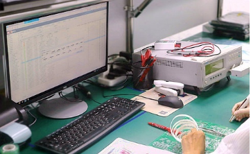
(1)Purpose:
Verify that raw materials (PCB substrates, electronic components, solder, etc.) meet specifications, performance, and reliability requirements.
(2)Inspection Content:
Component appearance (package, silk screen, lead oxidation), dimensions, and polarity;
Electrical parameters (resistance, capacitance, inductance, diode/transistor characteristics);
PCB substrate thickness, pad flatness, via quality, and surface coatings (solder mask, gold plating);
Material certification documents (RoHS compliance, batch consistency reports, OEM test reports).
2. Stencil Inspection
(1)Purpose:
Ensure cleanliness, opening precision, and tension of SMT solder paste stencils meet process requirements.
(2)Inspection Content:
Consistency of stencil opening dimensions with design files (aperture size, shape, positional deviation);
Residual solder paste or contaminants on the stencil surface;
Stencil tension (measured via tensiometer for printing stability).
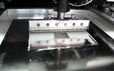
3. Solder Paste Inspection (SPI)
(1)Purpose:
Monitor solder paste printing quality to avoid soldering defects (insufficient solder, excessive solder, misalignment, bridging).
(2)Inspection Content:
Solder paste thickness, volume, position, and shape;
Printing misalignment (alignment relative to PCB pads);
Edge clarity and presence of bridging.
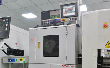
4. In-line Automated Optical Inspection (In-line AOI)
(1)Purpose:
Detect surface mount defects immediately after reflow soldering for real-time process feedback.
(2)Inspection Content:
Missing/misplaced components, polarity reversal, tombstoning, skewing;
Solder joint defects (insufficient/excessive solder, bridging, pad contamination);
Lead deformation or pad damage.
5. SMT First Article Inspection (FAI)
(1)Purpose:
Validate the correctness of the first assembled PCBA before mass production to prevent batch errors.
(2)Inspection Content:
Component designator, type, package, and polarity against BOM;
Placement precision (X/Y offset, rotation angle);
Pad coverage and lead coplanarity (for QFP, BGA, etc.).


评论
发表评论