PCB Panelization: Boost Efficiency & Cut Costs
In the fast-paced world of electronics, efficiency and cost-effectiveness are paramount. Printed Circuit Boards (PCBs) are the foundation of virtually all electronic devices, and their manufacturing process is a complex dance of precision and speed. One crucial technique that significantly streamlines this process is PCB panelization. This method is the unsung hero behind mass-produced electronics, transforming individual board fabrication into a highly efficient, assembly-line operation.
PCB panelization, often referred to as PCB array or PCB nesting, involves arranging multiple individual PCBs onto a larger, single panel. This panel is then processed as a single unit throughout various stages of fabrication and assembly, rather than handling each board separately. The result? A dramatic reduction in manufacturing time, material waste, and overall production costs. Whether you’re a seasoned PCB designer or a manufacturer looking to optimize your workflow, understanding the nuances of panelization is key to unlocking greater productivity and profitability.
1. What is PCB Panelization?
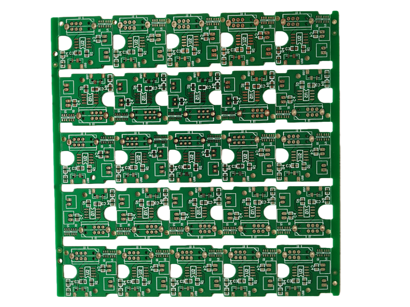
PCB panelization is a manufacturing practice where several individual printed circuit boards are grouped together onto a larger substrate, known as a panel or array, for simultaneous production. Instead of manufacturing and assembling each board independently, multiple identical or even different board designs are fabricated as a single unit. After all manufacturing and assembly processes are complete, these individual PCBs are then separated from the panel along pre-defined lines.
This method is widely adopted in high-volume PCB manufacturing due to its ability to drastically improve efficiency. By treating an array of boards as one, factories can maximize the use of their equipment, such as pick-and-place machines for automated assembly, reflow ovens, and soldering systems . This centralized processing minimizes the number of times equipment needs to be set up or reconfigured, thereby saving valuable time and labor. The ultimate goal of panel design is to optimize the manufacturing process from start to finish, ensuring a smooth transition through each stage of production.
2. Why Panelize? Unpacking the Benefits
The importance of PCB panelization cannot be overstated for modern PCB manufacturing and PCB assembly. It offers a multitude of advantages that directly impact a project’s bottom line and timeline. Here are the primary benefits:
- Enhanced Efficiency and Throughput:By processing multiple boards concurrently, manufacturers can achieve higher production volumes in less time. This parallel processing significantly reduces cycle times, making it ideal for large-scale production runs and improving the overall efficiency of the assembly line.
- Significant Cost Reduction:Cost reduction is perhaps the most compelling benefit. Panelization minimizes setup times for machinery, reduces material handling costs, and optimizes the use of raw materials by tightly nesting designs. This economy of scale translates to lower per-board production costs, making projects more competitive.
- Improved Handling in Automated Assembly:Individual small PCBs can be difficult to handle with automated assembly equipment. A larger, rigid panel provides a stable substrate that is easier to transport, load into machines, and manage throughout the assembly process. This reduces the risk of damage and ensures consistent placement.
- Reduced Material Waste:Intelligent panel design allows for better utilization of raw PCB laminate material. By arranging multiple boards, designers can minimize the unused space on a panel, leading to less scrap material and greater sustainability.
- Consistent Quality and Reliability:Processing boards in a panel ensures that each unit undergoes the same manufacturing conditions simultaneously. This consistency helps in maintaining uniform quality across all boards, reducing variations that might occur if each board were processed individually.
- Streamlined Testing:A panel can often be tested as a whole or in sections before individual boards are broken apart. This can simplify and speed up functional testing, further contributing to efficiency.
Ultimately, panelization is a strategic choice that boosts manufacturing capabilities, cuts expenses, and ensures the reliability of the final electronic product.


评论
发表评论